100nmサイズの微細加工を施したフォトニック結晶を波長385nmの紫外線LED上に作製することに成功し、光閉じ込め効果を確認しました。
弊社は、波長385nmの紫外線LED (以下UV-LED)上に、100nmサイズの微細加工を施したフォトニック結晶(Photonic crystal 以下PhC)を作製し、光閉じ込め効果を確認しました。フォトニック結晶とは、屈折率が周期的に変化する構造で、光を小さな領域に閉じ込め、光と物質の相互作用を高めることに利用されています。光の波長に適合したサイズの周期構造を人工的に作れば、通常の物資では不可能な光学的性質を持つメタ物質を実現することができます。近年、半導体微細加工技術の進歩により、光スイッチ、レーザ、光メモリ、レーザ光源といった光デバイスに於いて、低消費電力での基本動作が確認されています。
PRESS RELEASE
マスコミの皆様
令和5年5月10日
ナイトライド・セミコンダクター株式会社
代表取締役 村本 宜彦
◆
概要
弊社は、波長385nmの紫外線LED(以下UV-LED)上に100nmサイズの微細加工を施したPhotonic Crystalフォトニック結晶(以下PhC)の開発に成功し、光閉じ込め効果を確認しましたので、ご報告申し上げます。
◆
背景
フォトニック結晶とは、屈折率が周期的に変化する構造で、光を小さな領域に閉じ込め、光と物質の相互作用を高めることに利用されています。光の波長に適合したサイズの周期構造を人工的に作れば、通常の物資では不可能な光学的性質を持つメタ物質を実現することができます。近年、半導体微細加工技術の進歩により、光スイッチ、レーザ、光メモリ、レーザ光源といった光デバイスに於いて、低消費電力での基本動作が確認されています。
(NTT研究開発Web参照)
◆
意義
発光ダイオード(以下LED)の光は、発光層に於いて発光し、全方位360°に光が照射されるので、チップ内部のリフレクター構造によって、前面から光を取り出します。LEDチップは、すり鉢状のパッケージに実装され、更に、光学レンズによって、指向角を狭くすることで、照射範囲をコントロールします。紫外線は、樹脂、ガラスに吸収されるため、石英等のUV透過率の高い光学レンズが使用されますが、コストが高いこと、レンズと半導体材料の屈折率差による損失が発生するため、効率が悪化します。そこで、レンズを用いないで、指向角を制御するUV-LEDが待望されています。
◆
応用
UV-LEDは、有害物質を含まないクリーンな半導体製造用光源として、紫外線(水銀)ランプに置き換わることが期待されています。UV-LEDにフォトニック結晶加工を施すことで、高効率、省エネ、環境に優しいUV光源が実現できます。また、近年、開発が活発になっているマイクロLEDディスプレイ用光源として、UV-LEDとRGB蛍光体を組み合わせてフルカラーを得る方式のディスプレイの開発が進んでいます。マイクロサイズのUV-LEDチップが発する光を光学レンズで制御することは、コストが高くなるばかりでなく、微細なレンズアレイを製作することが困難です。そこで、フォトニック結晶を利用することで、安価に効率的に光を制御することができます。
その他、UV-LEDに限らず、LED照明に応用される青色LEDにフォトニック結晶加工を施すことで、現在のLED照明よりも、高輝度で、低消費電力の照明を安価に実現できます。
◆
Photo
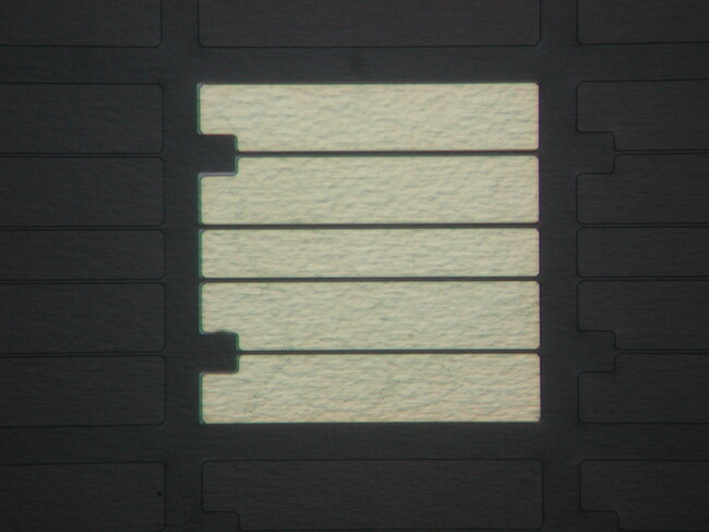
385nmUV-LEDチップ上のPhCが白色照明光を閉じ込めて発光している様子(未通電時)
On the 385nm UV-LED chip, PhC emits light by confining white light (when power is off)
Press Release
To members of the media
May 10, 2020
Nitride Semiconductor Co., Ltd.
Founder, President & CEO
Yoshihiko Muramoto
◆Overview
We have succeeded to develop the Photonic Crystal (hereinafter referred to as PhC) on which 100 nm size nanofabrication is performed on an ultraviolet LED (hereinafter referred to as UV-LED) with a wavelength of 385nm. We confirmed the light confinement effect of the PhC.
◆ Background
A photonic crystal is a structure in which the refractive index changes periodically and is used to confine light in a small area and enhance the interaction between light and matter. By artificially creating a periodic structure with a size that matches the wavelength of light, it is possible to realize metamaterials with optical properties that are not possible with ordinary materials. In recent years, due to advances in semiconductor microfabrication technology, basic operation with low power consumption has been confirmed in optical devices such as optical switches, lasers, optical memories, and laser light sources.
(Refer to NTT R&D website)
◆ Significance
Light from a light-emitting diode (hereinafter referred to as LED) is emitted from the active layer, and the light is emitted 360 degrees in all directions, so the reflector structure inside the chip extracts the light from the front. The LED chip is mounted in a cup-shaped package, and an optical lens narrows the directional angle to control the irradiation range. UV rays are absorbed by resin and glass, so optical lenses with high UV transmittance, such as quartz, are used. Therefore, there is a long-awaited UV-LED that controls the directivity angle without using a lens.
◆ Application
UV-LED is expected to replace ultraviolet (mercury) lamps as a clean light source for semiconductor manufacturing that does not contain harmful substances. By applying photonic crystal processing to UV-LEDs, highly efficient, energy-saving, and environmentally friendly UV light sources can be realized. In addition, as a light source for micro-LED displays, which have been actively developed in recent years, the development of full-color displays by combining UV-LEDs and RGB phosphors is progressing. Optical lens control of the light emitted by a micro-sized UV-LED chip not only increases the cost, but also makes it difficult to fabricate a fine lens array. Therefore, by using photonic crystals, light can be controlled efficiently at low cost.
In addition to UV-LEDs, by applying photonic crystal processing to blue LEDs that are applied to LED lighting, it is possible to realize lighting with higher brightness and lower power consumption than current LED lighting at a low cost.